Today’s Wafer Designs Put Premium on Precision— 300i Increases ROI
Value of incoming wafer inspection with 300i’s ±0.25µm accuracy far outweighs potential for costly downstream yield losses
LOCKPORT, IL, UNITED STATES, December 17, 2025 /EINPresswire.com/ -- Semiconductor fabrication facilities risk substantial financial exposure from incoming wafers defects. With typical lot sizes of 25 wafers and finished wafer values ranging from $4,000 to $17,000, depending on complexity, a single contaminated lot can translate into $100,000 to $425,000 in processed material losses – plus the costs of production delays, Vitrek’s affordable Proforma 300i manual metrology system, provides the precision needed to insure y against costly defects with superior pre-process testing.The Hidden Cost of Minute Incoming Wafer Defects
Thickness variations, and flatness deviations that are virtually invisible to the naked eye can translate into accumulated tolerance issues after the stress of multiple thermal cycles and material deposition processes. These issues can translate into lithography focus errors, process uniformity problems, and even mechanical handling failures that cause a tool to enter an error state or compromise the number of usable chips per wafer.
“The substrate cost is a fraction of the total finished wafer value,” said Dan Melchior, Sales Manager for Semiconductor Products at Vitrek. “When bare wafer defects trigger yield loss after multiple process steps, recovery costs from a single compromised lot can reach six figures. The Proforma 300i offers the accuracy needed to catch these issues before a wafer enters the fab process”.
Industry data confirms that proactive incoming inspection delivers measurable ROI. Facilities processing 1,000 wafers monthly that prevent even one defective lot quarterly through systematic incoming inspection can avoid $400,000 to $1.7 million in annual exposure, far exceeding the costs of an early detection metrology system like the 300i.
Precision Capacitance Measurement for Critical Parameters
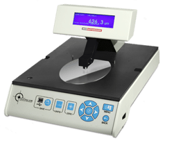
The Proforma 300i uses Vitrek’s proprietary capacitance-based technology for non-contact, and non-destructive wafer geometry inspection. It measures thickness and TTV with ±0.25µm accuracy and 0.05µm resolution and performs bow and flatness assessments to detect stress and surface variations during in-process testing.
Its non-contact design works effectively with materials like silicon, GaAs, InP, and sapphire, and supports wafer sizes from 76mm to 300mm. Proprietary sensor technology ensures high accuracy without the presence of an electrical ground. With a 16.6Hz measurement frequency, the Proforma 300i enables fast, high-volume inspections. USB and Ethernet connectivity allows for easy data collection for lot-to-lot tolerance comparisons.
Protecting Process Equipment from Defective Wafers
“Process equipment protection is arguably more critical than material loss prevention,” noted Melchior. “A defective wafer that compromises a lithography tool can result in unplanned cleaning cycles at downtime costs of tens of thousands of dollars per hour, plus repair expenses that can reach six figures for advanced systems. The Proforma 300i’s precision geometry measurement can safeguard against both wafer yield losses and capital equipment maintenance investments. We have prototypes for sensors and amplifiers that are even more precise than our most popular wafer measurement products, but we have not been pushed to deliver them.
Supplier Validation and Quality Assurance
The non-contact Proforma 300i scans each wafer comprehensively, eliminating the need for sampling or destructive analysis. It works without compromising the wafer surface, reducing sample waste and better aligning processes with both efficiency and sustainability goals.
About Vitrek, LLC and the MTI Instruments Line of Metrology Tools
Vitrek makes and sells a variety of tools for semiconductor manufacturers under the MTI Instruments brand. These include the best-in-class Accumeasure™ capacitance probe sensors and PCB-based amplifiers as well as their Protrak™ laser profile sensors. Vitrek’s product portfolio also includes Vitrek hipot testers and power analyzers as well as the GaGe high-resolution, high-speed digitizer cards, which are used for semiconductor packaging as well as wafer production.
Sam Cremin
Vitrek
+1 8158380005
email us here
Legal Disclaimer:
EIN Presswire provides this news content "as is" without warranty of any kind. We do not accept any responsibility or liability for the accuracy, content, images, videos, licenses, completeness, legality, or reliability of the information contained in this article. If you have any complaints or copyright issues related to this article, kindly contact the author above.
